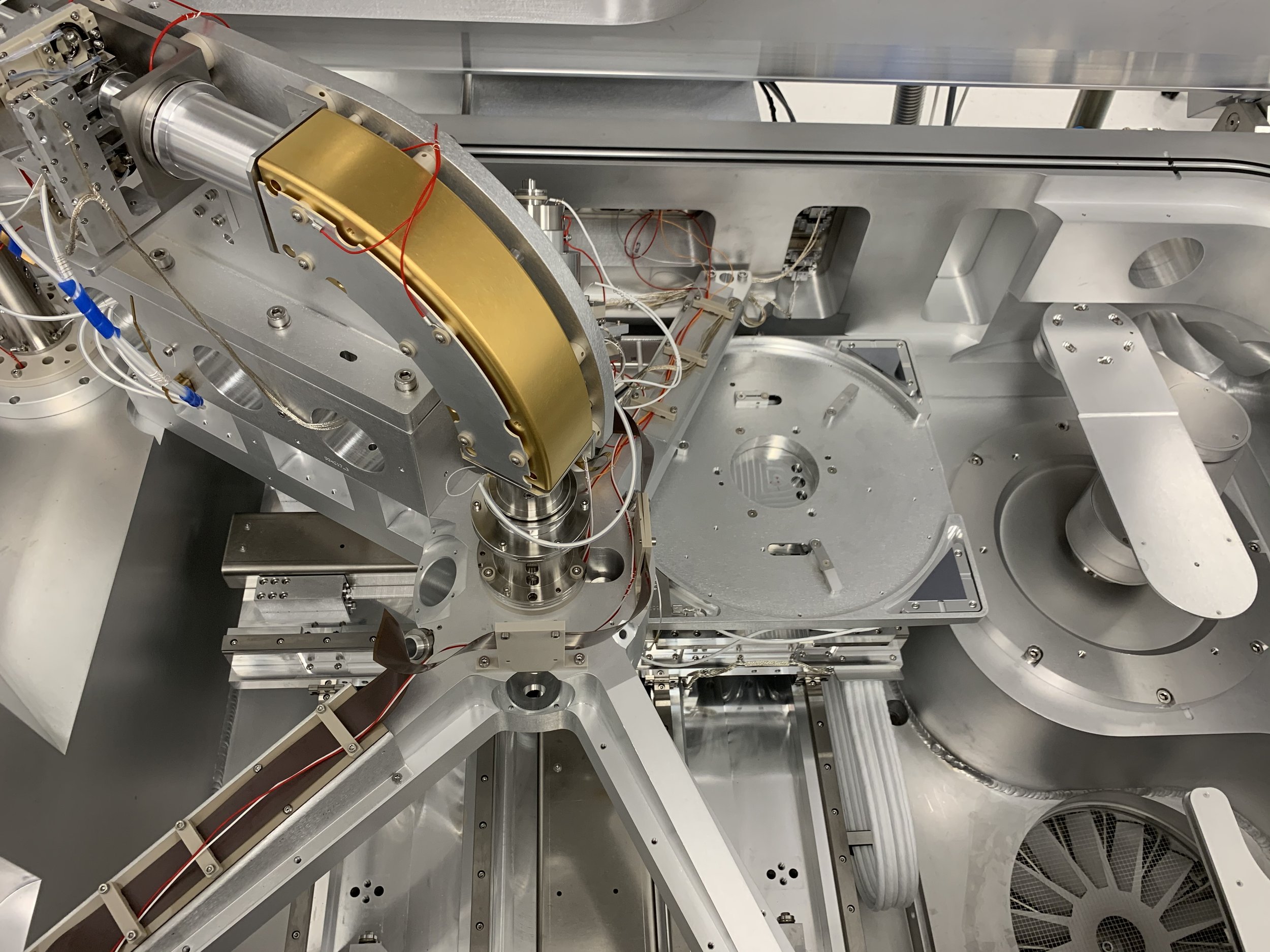
The challenge: Secondary Ion Mass Spectrometry (SIMS) had always been a lab technique — too slow and delicate for a semiconductor production line. Our client wanted to change that: a second-generation SIMS tool that could run in-line, in production, measuring multiple elements at once. Nothing like it existed.
What we designed: The mechanical architecture for the world’s first in-line SIMS production inspection tool — which also debuted as the world’s first multi-element inspection tool. The system used a radio-frequency-generated plasma and required designing every component for an ultra-high vacuum (UHV) scanning environment: material selection, venting, surface finish, and sealing all driven by vacuum compatibility.
We also analyzed the 400 lb. lid/optics assembly of an X-ray spectroscopy inspection tool using FEA and free-body diagrams, validating operator safety for certification. And we managed the top-level SolidWorks assemblies for both tools — the SIMS assembly was the largest file our SolidWorks distributor had ever seen — while overseeing the software and Vault migration.
The skills involved: Ultra-high vacuum design, spectroscopy instrument architecture, FEA safety analysis, large-assembly CAD management, semiconductor capital equipment design.
Designing for vacuum or semiconductor production? Contact us to discuss your tool architecture.